M199 - M-Module USM FPGA Development Kit (Product Discontinued)

USM Universal Submodules make M-Modules more flexible, cost and time-saving than ever. A main M-Module gets its specific function through the IP cores implemented inside its onboard FPGA. This function can be changed at any time through implementation ofdifferent IP cores. The corresponding line drivers are realized on a USM which is simply plugged on the main M-Module.

This FPGA USM development kit for M-Modules has been prepared for users who like to write and/or implement specific IP cores on their own. Even the growing range of Wishbone-based standard IP cores from duagon (different UARTs, Ethernet, fieldbus interfaces, graphics, digital I/O etc.) can be combined with your own or third-party functions.

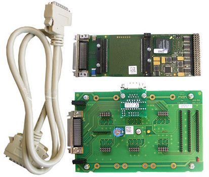
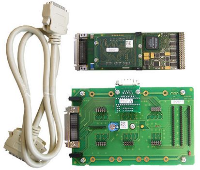
The kit includes the main M-Module M199 equipped with an FPGA, 32 MB DDR2 SDRAM, 8 MB Flash and a 50-pin SCSI connector. In addition the package includes a bare USM module, a test board where I/O signals from the FPGA are led to and where an additional debug interface is implemented, and a SCSI cable for connection between the main M-Module and test board. The Nios processor, memory control, and the Avalon/Wishbone bridges are installed on the main module. The corresponding FPGA development package is available as web download. For development of IP cores on the standard Wishbone bus the Wishbone Bus Maker tool from duagon is included. In order to use the Nios cores and to develop IP cores on the Avalon bus Altera's Quartus II design environment including the SOPC builder is needed separately.

ANSI standard mezzanine M-Modules can be used as an I/O extension in any type of bus system, i.e. CPCI, VME or on any type of stand-alone SBC. Appropriate M-Module carrier cards in 3U, 6U and other formats are available from duagon or other manufacturers.

Once a USM module has been developed for M-Modules, it may also be used on PMC or XMC and conduction-cooled PMC base modules, and vice versa.

Features

  • 1 Main M-Module M199 for USM Universal Submodules:
  • 1 FPGA 33,216 LE
  • 32 MB DDR2 SDRAM, 8 MB Flash
  • 1 bare USM module US0
  • 1 evaluation board with RS232 debug interface
  • 1 FPGA development package:
  • Main bus interface
  • Memory control
  • Nios softcore
  • Wishbone/Avalon bridges
  • For user-defined I/O
  • 1 SCSI cable
  • -40 to +85 °C with qualified components